


Breaking News
 "SPIRITS TOLD US" – Chief Says NO PROOF NEEDED For 215 KAMLOOPS GRAVES!!
 Financial Repression: How the US Government Will Quietly Confiscate Your Wealth
 U.S. Troops' Death Means "All Out War" with Iran!
 One of the Greatest Betrayals of Public Trust in American History
Top Tech News
 Anthropic is launching its own drug discovery programs for rare diseases using Claude...
 SpaceX AI Satellites Will Have 250 Kilowatts of Power
 Chinese researchers have developed a sodium-metal battery that can fully charge in just 4 minutes...
 SpaceX Starship Flight 13 in 3 Days - Thursday July 13
 Chinese Scientists Develop Nuclear Battery Using Carbon-14
 Teleoperated humanoid robots complete first-ever live surgery
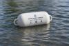 Floating capsule auto-disinfects water without chemicals or battery
 Modular Reactors To Solve Data Center Hysteria?
 DeepSeek Developing In-House AI Chip In Bid To Cut Nvidia Reliance
 America just took three brand-new nuclear reactors critical in thirty days, a first for any...


Laser-driven Particle Accelerator Made Ten Thousand Times Smaller
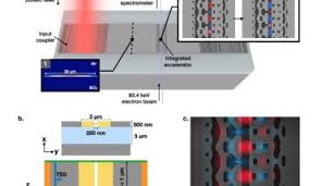
Current implementations of DLAs rely on free-space lasers directly incident on the accelerating structures, limiting the scalability and integrability of this technology. Researchers present the first experimental demonstration of a waveguide-integrated DLA, designed using a photonic inverse design approach. These on-chip devices accelerate sub-relativistic electrons of initial energy 83.4 keV by 1.21 keV over 30 µm, providing peak acceleration gradients of 40.3 MeV/m. This progress represents a significant step towards a completely integrated MeV-scale dielectric laser accelerator.
Dielectric laser accelerators have emerged as a promising alternative to conventional RF accelerators due to the large damage threshold of dielectric materials the commercial availability of powerful NIR femtosecond pulsed lasers, and the low-cost high-yield nanofabrication processes which produce them. Together, these advantages allow DLAs to make an impact in the development of applications such as tabletop free-electron-lasers, targeted cancer therapies, and compact imaging sources.