


Breaking News
People Who Weaved Themselves into the Tapestry of Your Life
 Rep. Massie Proposes NDAA Amendment Preventing Integration of IDF with US Military
 Liberals Have Relaxed About Trump Because They Trust Him To Keep the Wars Going
 LIVE Coverage of President Trump's Historic Speech Exposing Communist Chinese & Their Allies'
Top Tech News
 Chinese researchers have developed a sodium-metal battery that can fully charge in just 4 minutes...
 SpaceX Starship Flight 13 in 3 Days - Thursday July 13
 Chinese Scientists Develop Nuclear Battery Using Carbon-14
 Teleoperated humanoid robots complete first-ever live surgery
 Floating capsule auto-disinfects water without chemicals or battery
 Modular Reactors To Solve Data Center Hysteria?
 DeepSeek Developing In-House AI Chip In Bid To Cut Nvidia Reliance
 America just took three brand-new nuclear reactors critical in thirty days, a first for any...
 Your brain doesn't peak in your 20s after all: Study reveals your mind is at its sharpest betwee
 Compasses, not maps: China is building a different type of AI


Taiwan Semiconductor will have volume production of 7 nanometer chips...
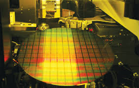
The foundry also described enhancements to its two chip-stacking techniques, advances in RF CMOS and work in transistors and materials, paving the way to a 3nm node and beyond. In addition, it previewed design capabilities using machine learning that it will offer before the end of the year.
Among its achievements, TSMC noted 76 percent yields on the 256Mbit SRAM made in its first-generation 7nm node, which will be in volume production next year. It also reported that an ARM Cortex-A72 processor in the node exceeded 4GHz using a new design flow.
The Taiwan company, already the world's largest foundry by far, expects to ship 11 million 12-inch-equivalent wafers this year, a typical 10 percent annual increase. The biggest share—two million wafers—will use its planar 28nm processes for which it is boosting capacity 15 percent this year.