


Breaking News
People Who Weaved Themselves into the Tapestry of Your Life
 Rep. Massie Proposes NDAA Amendment Preventing Integration of IDF with US Military
 Liberals Have Relaxed About Trump Because They Trust Him To Keep the Wars Going
 LIVE Coverage of President Trump's Historic Speech Exposing Communist Chinese & Their Allies'
Top Tech News
 Chinese researchers have developed a sodium-metal battery that can fully charge in just 4 minutes...
 SpaceX Starship Flight 13 in 3 Days - Thursday July 13
 Chinese Scientists Develop Nuclear Battery Using Carbon-14
 Teleoperated humanoid robots complete first-ever live surgery
 Floating capsule auto-disinfects water without chemicals or battery
 Modular Reactors To Solve Data Center Hysteria?
 DeepSeek Developing In-House AI Chip In Bid To Cut Nvidia Reliance
 America just took three brand-new nuclear reactors critical in thirty days, a first for any...
 Your brain doesn't peak in your 20s after all: Study reveals your mind is at its sharpest betwee
 Compasses, not maps: China is building a different type of AI


IBM has made Carbon nanotubes transistors smaller and faster than silicon
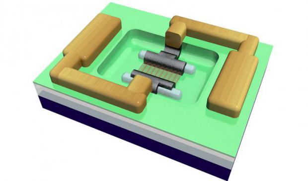
Now IBM and others will have to scale up superior carbon nanotube devices.
IBM scientists have been experimenting with carbon nanotubes, rolled-up sheets of carbon atoms just 1 nanometer, or a billionth of a meter, in diameter. But difficulties working with the material have meant that, for optimal performance, nanotube transistors have to be even larger than current silicon transistors, which are about 100 nanometers across. To cut that number down, a team of scientists used a new technique to build the contacts that draw current into and out of the carbon nanotube transistor. They constructed the contacts out of molybdenum, which can bond directly to the ends of the nanotubes, making them smaller. They also added cobalt so the bonding could take place at a lower temperature, allowing them to shrink the gap between the contacts. Another advance allowed for practical transistors.