


Breaking News
 Rep. Massie Proposes NDAA Amendment Preventing Integration of IDF with US Military
 Liberals Have Relaxed About Trump Because They Trust Him To Keep the Wars Going
 LIVE Coverage of President Trump's Historic Speech Exposing Communist Chinese & Their Allies'
 The Next Recession? What Americans Need To Know |Jiang Xueqin Explainer
Top Tech News
 Chinese researchers have developed a sodium-metal battery that can fully charge in just 4 minutes...
 SpaceX Starship Flight 13 in 3 Days - Thursday July 13
 Chinese Scientists Develop Nuclear Battery Using Carbon-14
 Teleoperated humanoid robots complete first-ever live surgery
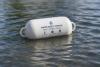 Floating capsule auto-disinfects water without chemicals or battery
 Modular Reactors To Solve Data Center Hysteria?
 DeepSeek Developing In-House AI Chip In Bid To Cut Nvidia Reliance
 America just took three brand-new nuclear reactors critical in thirty days, a first for any...
 Your brain doesn't peak in your 20s after all: Study reveals your mind is at its sharpest betwee
 Compasses, not maps: China is building a different type of AI


Ion beam controlled to etch single silicon atom depth
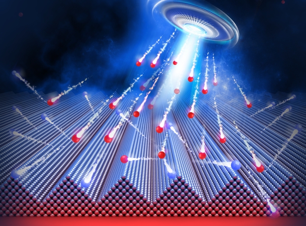
The beams can create tiny features in the lateral dimensions—length and width, but to create the next generation of nanometer-scale devices, the energetic ions must precisely control the features in the vertical dimension—depth. Now, researchers at the National Institute of Standards and Technology (NIST) have demonstrated that a standard ion-beam technique can be fine-tuned to make structures with depths controlled to within the diameter of a single silicon atom.
Above – nanofluidic staircase machined with subnanometer precision by a focused ion beam separates nanoparticles by size. The device is also a reference material to accurately measure nanoparticle size and compare it to optical brightness, which could aid in the quality control of consumer products. Credit: NIST