


Breaking News
 #662: Groomed Into Submission
 Tucker Carlson: Americans have a right to feel betrayed
 The Cult Around Israel No One Wants to Talk About
 You fill your car with gasoline
Top Tech News
 Anthropic is launching its own drug discovery programs for rare diseases using Claude...
 SpaceX AI Satellites Will Have 250 Kilowatts of Power
 Chinese researchers have developed a sodium-metal battery that can fully charge in just 4 minutes...
 SpaceX Starship Flight 13 in 3 Days - Thursday July 13
 Chinese Scientists Develop Nuclear Battery Using Carbon-14
 Teleoperated humanoid robots complete first-ever live surgery
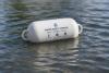 Floating capsule auto-disinfects water without chemicals or battery
 Modular Reactors To Solve Data Center Hysteria?
 DeepSeek Developing In-House AI Chip In Bid To Cut Nvidia Reliance
 America just took three brand-new nuclear reactors critical in thirty days, a first for any...


Breakthrough could triple the energy collected by solar to 60% efficiency
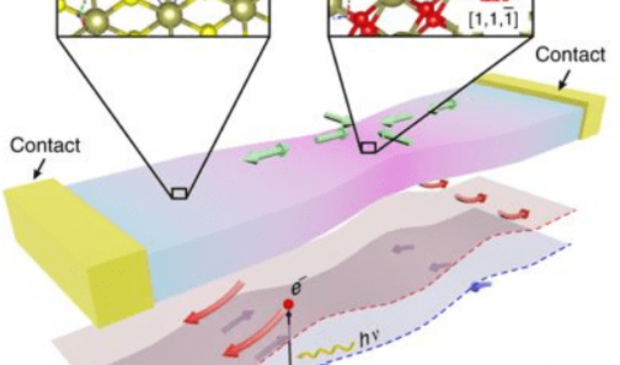
UK researchers can now 'funnel' electrical charge onto a chip. Using the atomically thin semiconductor hafnium disulphide (HfS2), which is oxidized with a high-intensity UV laser, the team were able to engineer an electric field that funnels electrical charges to a specific area of the chip, where they can be more easily extracted.
This method has the potential to harvest three times the energy compared with traditional systems. The researchers believe their breakthrough could result in solar panels, no bigger than a book, producing enough energy to power a family-sized house.

Abstract – Strain-engineered inverse charge-funnelling in layered semiconductors
The control of charges in a circuit due to an external electric field is ubiquitous to the exchange, storage and manipulation of information in a wide range of applications. Conversely, the ability to grow clean interfaces between materials has been a stepping stone for engineering built-in electric fields largely exploited in modern photovoltaics and opto-electronics.