


Breaking News
 Rand Paul voted to merge the United States military with Israels.
 GeoJourney 11| Inside the Build: Stage Four Begins
 Car Mechanics Are Quitting Everywhere - Nobody Wants These Jobs in 2026
 Eight babies born after Mitochondrial donation (This. Is. Not. Good.)
Top Tech News
 Chinese researchers have developed a sodium-metal battery that can fully charge in just 4 minutes...
 SpaceX Starship Flight 13 in 3 Days - Thursday July 13
 Chinese Scientists Develop Nuclear Battery Using Carbon-14
 Teleoperated humanoid robots complete first-ever live surgery
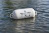 Floating capsule auto-disinfects water without chemicals or battery
 Modular Reactors To Solve Data Center Hysteria?
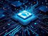 DeepSeek Developing In-House AI Chip In Bid To Cut Nvidia Reliance
 America just took three brand-new nuclear reactors critical in thirty days, a first for any...
 Your brain doesn't peak in your 20s after all: Study reveals your mind is at its sharpest betwee
 Compasses, not maps: China is building a different type of AI


TSMC will starting full EUV lithography of 5 nanometer chips April 2019
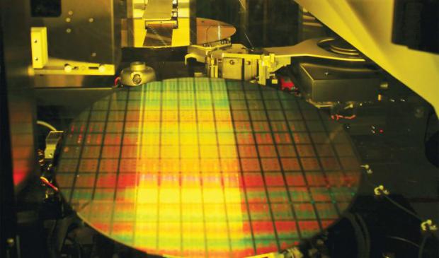
The foundry's update showed that area and power gains continue in its leading-edge nodes, but chip speeds are no longer advancing at their historic rate. To compensate, TSMC gave an update on a half-dozen packaging techniques that it is developing to speed connections between chips.
The TSMC N7+ node that can use EUV on up to four layers. Its N5 that will use EUV on up to 14 layers will be ready for risk production in April. EUV aims to lower costs by reducing the number of masks required for leading-edge designs.
Samsung is ramping a 7-nm node using EUV. Intel is not expected to use EUV anytime soon. Globalfoundries announced in August that it has halted work on 7 nm and EUV.