


Breaking News
 UPDATE: Netanyahu Declares Israel Will Not Comply With Lebanese Portion Of Peace Deal
 At Least Five Killed as Israel Continues To Pound Southern Lebanon
 America's Hidden Food Crisis and the Fear of Confiscation
 Trump: Iran Deal to Be Inked on Sunday Ahead of G7
Top Tech News
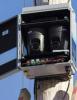 Heads up: Apparently the government is hiding cameras inside fake utility boxes
 Sodium Batteries And EVs That Power The Grid: Inside GM's Big Energy Push
 NUCLEAR ENGINE - UNLIMITED LUXURY - 20 YEARS WITHOUT REFUELING
 China Unveils Nuclear-Powered Floating Hub For Green Shipping
 China Launches World's 1st Commercial Brain Chip, Beating Elon Musk's Neuralink!
 Modular next-gen US nuclear reactor goes critical
 How EMF's cause disease
 This Company Will Add Phone, AirPod, and Smartwatch Trackers to License Plate Readers
 Elon Details SpaceX AI Data Center in Space Details and Roadmap
 5-in-1 miniature surgical robot is the size of a seed


TSMC 7+ Nanometer Chips Are in High Volume Production With 5, 6 nm in 2020
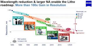
The N7+ process with EUV technology is built on TSMC's successful 7nm node and paves the way for 6nm and more advanced technologies.
The leading edge is currently at 7+ with about three layers done using EUV. In 2020, TSMC will ramp 5nm in the second half with significantly increased EUV usage of about 15 layers, followed by 6nm ramping at the end of 2020 with about four layers done in EUV, according to Jim Fontanelli, a senior analyst with Arete Research.
N7+ is also providing improved overall performance. When compared to the N7 process, N7+ provides 15% to 20% more density and improved power consumption, making it an increasingly popular choice for the industry's next-wave products. TSMC has been quickly deploying capacity to meet N7+ demand that is being driven by multiple customers.