


Breaking News
 Rand Paul voted to merge the United States military with Israels.
 GeoJourney 11| Inside the Build: Stage Four Begins
 Car Mechanics Are Quitting Everywhere - Nobody Wants These Jobs in 2026
 Eight babies born after Mitochondrial donation (This. Is. Not. Good.)
Top Tech News
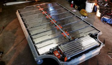
 Chinese researchers have developed a sodium-metal battery that can fully charge in just 4 minutes...
 SpaceX Starship Flight 13 in 3 Days - Thursday July 13
 Chinese Scientists Develop Nuclear Battery Using Carbon-14
 Teleoperated humanoid robots complete first-ever live surgery
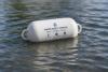 Floating capsule auto-disinfects water without chemicals or battery
 Modular Reactors To Solve Data Center Hysteria?
 DeepSeek Developing In-House AI Chip In Bid To Cut Nvidia Reliance
 America just took three brand-new nuclear reactors critical in thirty days, a first for any...
 Your brain doesn't peak in your 20s after all: Study reveals your mind is at its sharpest betwee
 Compasses, not maps: China is building a different type of AI


Finally, Commercialization of Wafers of Carbon Nanotube Transistor Chips
CNFETs are more energy-efficient than silicon field-effect transistors and could be used to build new types of three-dimensional microprocessors.
They found that dry cycling, a method of intermittently drying out the submerged wafer, could dramatically reduce the incubation time — from 48 hours to 150 seconds.
After analyzing the deposition technique used to make the CNFETs, Max Shulaker, an MIT assistant professor of electrical engineering and computer science, and his colleagues made some changes to speed up the fabrication process by more than 1,100 times compared to the conventional method, while also reducing the cost of production. The technique deposited carbon nanotubes edge to edge on the wafers, with 14,400 by 14,400 arrays CFNETs distributed across multiple wafers.
A 3D computer chip with combined logic and memory functions is projected to "beat the performance of a state-of-the-art 2D chip made from silicon by orders of magnitude.
Abstract
Carbon nanotube field-effect transistors (CNFETs) are a promising nanotechnology for the development of energy-efficient computing. Despite rapid progress, CNFETs have only been fabricated in academic or research laboratories. A critical challenge in transferring this technology to commercial manufacturing facilities is developing a suitable method for depositing nanotubes uniformly over industry-standard large-area substrates. Such a deposition method needs to be manufacturable, compatible with today's silicon-based technologies, and provide a path to achieving systems with energy efficiency benefits over silicon. Here, we show that a deposition technique in which the substrate is submerged within a nanotube solution can address these challenges and can allow CNFETs to be fabricated within industrial facilities.