


Breaking News
 "SPIRITS TOLD US" – Chief Says NO PROOF NEEDED For 215 KAMLOOPS GRAVES!!
 Financial Repression: How the US Government Will Quietly Confiscate Your Wealth
 U.S. Troops' Death Means "All Out War" with Iran!
 One of the Greatest Betrayals of Public Trust in American History
Top Tech News
 Anthropic is launching its own drug discovery programs for rare diseases using Claude...
 SpaceX AI Satellites Will Have 250 Kilowatts of Power
 Chinese researchers have developed a sodium-metal battery that can fully charge in just 4 minutes...
 SpaceX Starship Flight 13 in 3 Days - Thursday July 13
 Chinese Scientists Develop Nuclear Battery Using Carbon-14
 Teleoperated humanoid robots complete first-ever live surgery
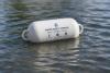 Floating capsule auto-disinfects water without chemicals or battery
 Modular Reactors To Solve Data Center Hysteria?
 DeepSeek Developing In-House AI Chip In Bid To Cut Nvidia Reliance
 America just took three brand-new nuclear reactors critical in thirty days, a first for any...


Taiwan Semiconductor Will Have Volume Production of 3 Nanometer Chips in 2022
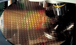
TSMC was the first company to use ASML's EUV lithography machines for high-volume production and now has at least three processes that use EUV for select layers. They use EUV lithography for its N7+, N6, and N5 nodes.
TSMC's 2nd generation 7 nm technology (N7+) uses EUV for up to four layers in order to reduce its use of multi-patterning techniques when building highly complex circuits. The 6 nm process (N6) is for customers to re-use IP designed for 1st generation 7 nm, per the report. TSMC's 5 nm process (N5) can use EUV for up to 14 layers. 5nm has significant increase in transistor density and performance enhancements.
2nd generation 5 nm (N5P) and 4 nm (N4) fabrication processes are based 5 nm technology and will have performance and power benefits. N5P will be available in 2021. N4 chips will have volume production in 2022.
Next-generation 3 nm process (N3) will be a full node improvement over N5. N3 will have 70 percent logic density gain, 15-percent performance gain, and 30-percent power reduction over the 5-nm process. N3 will use EUV over 20 layers.
Nextbigfuture covered Taiwan Semiconductors plans from 2017. TSMC has kept on track with its Moore's Law roadmap to reach 3-nanometer chips by 2022.