


Breaking News
 Frustrated Trump Vows To Hit Iranian Infrastructure - Will It Matter?
 "Being Stupid Feels Safe!" - News Update
 6.8 GW SHORT – The Valley Is The New Front Line In The AI Land Grab
 10/7: A Conspiracy Theory
Top Tech News
 Anthropic is launching its own drug discovery programs for rare diseases using Claude...
 SpaceX AI Satellites Will Have 250 Kilowatts of Power
 Chinese researchers have developed a sodium-metal battery that can fully charge in just 4 minutes...
 SpaceX Starship Flight 13 in 3 Days - Thursday July 13
 Chinese Scientists Develop Nuclear Battery Using Carbon-14
 Teleoperated humanoid robots complete first-ever live surgery
 Floating capsule auto-disinfects water without chemicals or battery
 Modular Reactors To Solve Data Center Hysteria?
 DeepSeek Developing In-House AI Chip In Bid To Cut Nvidia Reliance
 America just took three brand-new nuclear reactors critical in thirty days, a first for any...


IBM Efficient Silicon Waveguides Could Enable Revolutionary Photonic chips
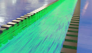
Above – Illustration of a pair of silicon high contrast gratings that can be used to guide visible light on a chip with low losses despite large absorption by the silicon material.
Nanostructures were used to make high contrast gratings. Such a grating consists of nanometer-sized 'posts' lined up to form a 'fence' that prevents light from escaping. The posts are 150 nanometers in diameter and are spaced so that light passing through them interferes destructively with light passing between them. Destructive interference is a phenomenon where waves – including electromagnetic waves such as visible light – that oscillate out of sync cancel each other out. This way, no light can "leak" through the grating and most of it gets reflected back inside the waveguide.
The next step is to engineer the efficient coupling of the light out of the waveguides into other components. That's a crucial step in our research, with the ultimate goal of integrating the all-optical transistors into integrated circuits that would be able to perform simple logic operations.